 EN
EN


Visit ALPHABETTER
I visited this company in Shenzhen. It's an excellent company, absorbing and learning from many advanced technologies and producing high-tech products. It's one of the leading enterprises representing new quality productivity – a high-quality domestic brand.
They are still striving to grow. It's a relatively new company, established in 2020.
They showed us great recognition and trust. I visited their production base, a facility worth hundreds of billions, with top-tier cleanrooms. They are a new, focused, and specialized enterprise, a "little giant" company, and will go public in the future. Last year, they raised $150 million.
Their products are mainly supplied to chip manufacturers, wafer foundries, panel manufacturers, BOE, TCL, and others for product testing at the 5-micron level. [For example, SMIC, TSMC, etc.] A single piece of equipment ranges from 3 million to 6 million RMB.
These are testing machines used on production lines.
The biggest takeaway is that professional competence is what large enterprises, platforms, and companies value most, as is a professional attitude.
The message is that it's not that they lack clients; rather, they are following the national direction of quality improvement and upgrading, producing more advanced products. We ourselves also need to strive to upgrade ourselves.
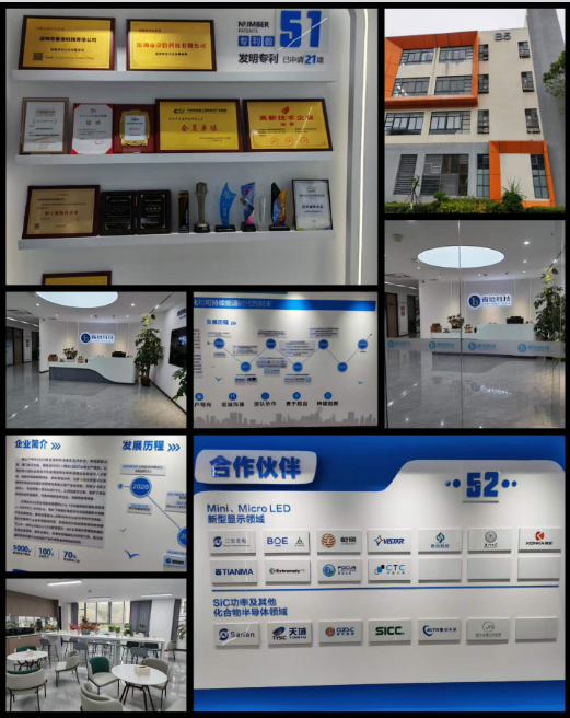
ALPHABETTER Technology was officially established in Bao'an District, Shenzhen in 2020, and subsequently set up branches in Shanghai and Xiamen, possessing a modern R&D and production base of nearly 5,000 square meters. The company's core team consists of high-level talents from renowned universities and semiconductor equipment companies both domestically and internationally, possessing R&D backgrounds and system engineering industrialization experience in semiconductor physics theory, materials characterization and analysis, self-developed high-end optical components, and precision electromechanical automation. Currently, the company has over 100 employees, with professional R&D personnel accounting for nearly 70%. Since its establishment, the company has received multiple rounds of external financing from well-known institutions and has won honors such as High-tech Enterprise and Specialized, Refined, and Innovative Enterprise. In 2022, the company released China's first Micro LED wafer-level mass inspection system, a-INSPECM1000e, filling the gap in domestic suppliers of front-end wafer inspection in the high-end optoelectronic display industry. Yibei Technology is committed to improving the process control and yield management of compound semiconductor substrates, epitaxy, and chips, based on materials analysis and spectral optics technologies. We provide quantitative, standardized, and intelligent testing tools for the booming advanced application fields such as Mini/Micro LED displays and SiC power devices, helping China's semiconductor equipment industry achieve its goal of upgrading from industrial to global leadership.
By the way, we offer professional international logistics, with stable air and sea freight services to Europe, America, the Middle East, and Southeast Asia. Our channels are reliable and our delivery times are guaranteed. Contact us anytime for your freight needs!